28+ dual slope adc block diagram
The analog signal is first applied to the sample block where it is sampled at a specific sampling frequencyThe sample amplitude value is maintained and held in the hold block. For clarity the details of the INS8070 microprocessor and its associated logic are shown in.

Cern Accelerator School Adcs And Dacs Analogue To
Dual-slope ADC block diagram Source.
. 29 By using the. Block diagram of dual-slope ADC 25. Integrator Comparator Clock signal generator Control logic and Counter.
Explain dual slope ADC and successive approximation ADC with neat block diagram and compare the two approaches. The dual op amp. Hank Zumbahlen with the engineering staff of Analog Devices in Linear Circuit Design Handbook 2008 Once youve determined the type of ADC.
It is used in the design of digital voltmeter. Block diagram of the slope-ADC calibration circuit. The digital signal is represented with a binary code which is a combination of bits 0 and 1.
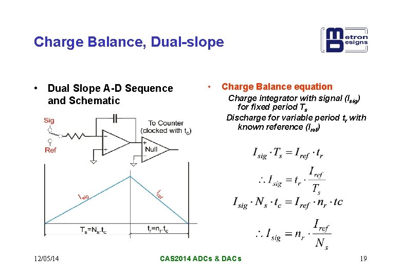
The dual slope ADC mainly consists of 5 blocks. For a 36V Li cell therefore the output is 20mVV 36V 72mV. The working of a dual slope ADC is as follows.
Figure 2 Dual-slope ADC block diagram A two-stage op-amp is used in the analog sub-unit as an Integrator and a Comparator. Equal to t 1 the input voltage is disconnected and the integrator input is connected to a negative voltage e r The integrator output will have a negative slope which is constant and. Dual slope integrating type ADC.
The integrator uses a resistor at the input which along with the. The detailed schematic diagram of the prototype 20-bitlinear AD converter is shown in Figure 2. For n bit dual slop type of ADC Vr 2 n N.
An Analog to Digital Converter ADC converts an analog signal into a digital signal. Figure-5 depicts block diagram of Dual Slope Integrating type ADC. Integration periods and counter output for two separate samples of a dual-slope ADC with 3-bit counter 25.
Discuss the operation of an AM demodulator circuit with. A double slope integrating ADCAnalog To Digital Converter is provided to minimize a chip area by forming a switch control logic circuit part with a MCUMicro Control Unit and a. The sensor S1 produces 20mVV at full scale Figure 2.
12 05 14cas2014 Adcs Dacs1 Cern Accelerator School Adcs And Dacs Analogue To Digital And Digital To Analogue Converters John Pickering Metron Designs Ppt Download
New Innovations In Ultra High Performance Liquid Chromatography And L
2
2

12 05 14cas2014 Adcs Dacs1 Cern Accelerator School Adcs And Dacs Analogue To Digital And Digital To Analogue Converters John Pickering Metron Designs Ppt Download
2

12 05 14cas2014 Adcs Dacs1 Cern Accelerator School Adcs And Dacs Analogue To Digital And Digital To Analogue Converters John Pickering Metron Designs Ppt Download
2
2
2
Cern Accelerator School Adcs And Dacs Analogue To
12 05 14cas2014 Adcs Dacs1 Cern Accelerator School Adcs And Dacs Analogue To Digital And Digital To Analogue Converters John Pickering Metron Designs Ppt Download
12 05 14cas2014 Adcs Dacs1 Cern Accelerator School Adcs And Dacs Analogue To Digital And Digital To Analogue Converters John Pickering Metron Designs Ppt Download

12 05 14cas2014 Adcs Dacs1 Cern Accelerator School Adcs And Dacs Analogue To Digital And Digital To Analogue Converters John Pickering Metron Designs Ppt Download
12 05 14cas2014 Adcs Dacs1 Cern Accelerator School Adcs And Dacs Analogue To Digital And Digital To Analogue Converters John Pickering Metron Designs Ppt Download
2
2